Signal Routing
Crosstalk in Microstrip Traces: What Causes Field Spread and How to Reduce It
What causes crosstalk and how to minimize field spread.
· 1 min read
Key takeaway
Crosstalk between microstrip traces comes from overlapping fields, and field spread on the reference plane falls off roughly as (h/x)². Increasing trace spacing is the most reliable fix; reducing dielectric height is a useful second lever on dense boards, with diminishing returns.
Crosstalk is defined by the fields, but where are the fields?
In a real PCB, crosstalk stems from overlapping electromagnetic fields between adjacent traces. While increasing physical trace separation is your primary and most reliable defense, optimizing dielectric height offers a powerful second lever to pull in your design.
To understand how these aspects influence the fields, let’s take a microstrip trace for example:
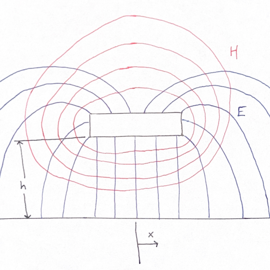
Remember that signal energy propagates as an electromagnetic wave through the dielectric space between the trace and its reference plane. The return current on the reference plane flows where these electric field lines terminate.
For a microstrip line, the return current density on the reference plane at a distance x relative to the trace centerline, with some assumptions, simplifies to (h²/x²), where h is the dielectric height and x is the distance from the trace centerline. Because crosstalk is directly proportional to this field spread, you have two choices:
• 𝗜𝗻𝗰𝗿𝗲𝗮𝘀𝗲 𝗧𝗿𝗮𝗰𝗲 𝗣𝗶𝘁𝗰𝗵 (𝘅): Spacing traces apart is the most effective way to reduce coupling, but it consumes PCB real estate.
• 𝗦𝗵𝗿𝗶𝗻𝗸 𝗗𝗶𝗲𝗹𝗲𝗰𝘁𝗿𝗶𝗰 𝗛𝗲𝗶𝗴𝗵𝘁 (𝗵): Decreasing laminate thickness tightly bounds the fields beneath the trace, suppressing field reach without widening trace pitch. Be aware, this will influence the trace width in a controlled impedance design.
A thinner dielectric is not a blanket fix. Shrinking dielectric height provides diminishing returns. Bringing a trace closer to the reference plane lowers return inductance, but it increases the plane’s AC resistance by squeezing return current into a narrower strip.
Below a certain height, depending on frequency, the spread of the fields can no longer be reduced. I suggest referencing Henry Ott’s book, Electromagnetic Compatibility Engineering, for a deeper explanation.
Physical separation is the best protection, but tuning dielectric height provides leverage on dense boards.